What is Efabless?
As quoted on the website,
“Efabless is a free cloud-based chip design platform, growing community of 1000+ chip designers, and fabrication friendly technology company that takes you from idea to silicon inside your product”.
Efabless not only facilitates opportunities to develop low-cost design but has indeed been known for promoting open-source practices in chip design, including providing an open-source design flow. The concept of an open-source design flow refers to making the entire process of designing a semiconductor chip accessible and transparent to the community.
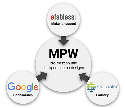
Make your custom chip for free!
Anyone can design and fabricate their open-source design for free with the Open MPW (Multi-Project Wafer) Program. The shuttle program lets designers try out new ideas without worrying about the cost of making them. It’s open to everyone, as long as their project is fully open source and meets certain requirements. Google covers the costs of making, packaging, evaluating, and shipping the projects in this program.
Through this blog, we will cover the comprehensive process of IC Design flow using Open-source tools, exploring each stage from conception to fabrication
We will initially pace through some VLSI jargon at the beginning. It’ll all click into place when we delve into the intricacies later on. So, buckle up 🙂
What is a PDK?
A Process Design Kit (PDK) is a comprehensive set of files, data, and tools provided by semiconductor foundries to assist chip designers in developing integrated circuits compatible with a specific manufacturing process. It encompasses technology files, design rules, device models, standard cell libraries, and simulation tools crucial for designing and verifying semiconductor components. While many PDKs are proprietary and specific to certain foundries, some open-source PDKs are freely available to the public. Notable examples include SkyWater PDK, associated with the SkyWater Technology Foundry, and GF180MCU, an open-source PDK that is a collaboration between Google and GlobalFoundries.
GDSII
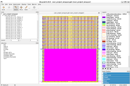
GDSII stream format (GDSII) is a binary database file format which is the de facto industry standard for data exchange of integrated circuit or IC layout artwork. It is a binary file format representing planar geometric shapes, text labels, and other information about the layout in hierarchical form. With the help of this file, the photomask is designed using a process called lithography. As shown in Figure 2 is a rendering of a small GDSII standard cell with three metal layers.GDSII files were originally written on magnetic tape. The final deadline for IC designers is still called tape-out for this reason!
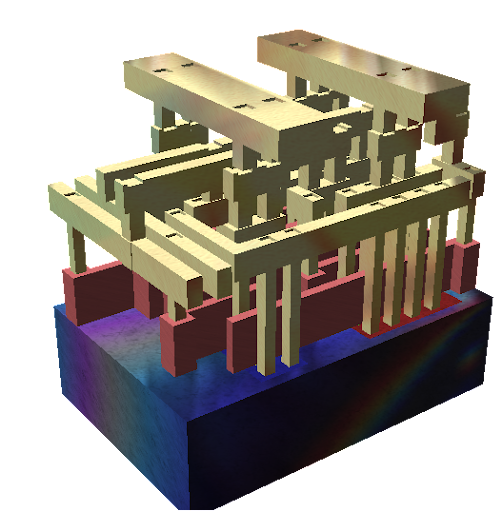
Source: Caravel Efabless
OpenLane
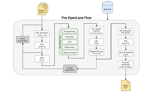
OpenLane is an open-source tool designed for implementing Application-Specific Integrated Circuits (ASICs). OpenLane is a no-human-in-the-loop RTL to GDS compiler built around OpenROAD that works like a GNU software compiler with trade-offs in area and performance. It simplifies the whole design flow from the high-level hardware description of the RTL Design to the Physical Design of the integrated circuit.
How does it work?
OpenLane operates on a straightforward yet efficient method based on modular “Steps” that can be combined to form “Flows.” Each Step has defined inputs and outputs, enabling the creation of highly complex chip layouts through their sequential chaining. Below are the steps in OpenLane flow.
Synthesis: The synthesis step converts a behavioural description of the design into an equivalent gate-level netlist. It then maps the functionality present in RTL code to the library of standard cells such as NAND, NOR… gates specific to the target technology node.
Static Timing Analysis: It checks the design for any timing violations ensuring that signals meet specified timing constraints and allowing designers to identify and address potential timing issues for optimal performance.
Floorplanning: This step involves arranging and optimizing the placement of digital components on a chip, determining their relative positions and sizes to meet design goals and constraints. Before placement, it is essential to determine the macro placement and blockages to ensure a compliant GDS file.
Placement: This step initially starts with a coarse placement of standard cells in roughly the right places, called global placement. The next step aligns the cells to the grid and ensures they don’t overlap while trying to reduce or limit the wiring length, which is a finer placement.
Routing: This step involves creating pathways for interconnections between standard cells on a chip, optimizing for signal integrity, and meeting design constraints.
Clock Tree Synthesis: This step generates a hierarchical tree structure for distributing clock signals, optimizing for low skew (variation in signal arrival time) and power consumption.
Design Rule Check: DRC (Design Rule Checking) verifies that the layout of an integrated circuit complies with predetermined manufacturing rules, ensuring error-free physical design. It is a pivotal step to identify and correct potential violations that could affect the functionality and reliability of the final chip.
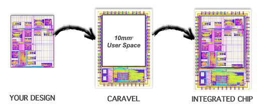
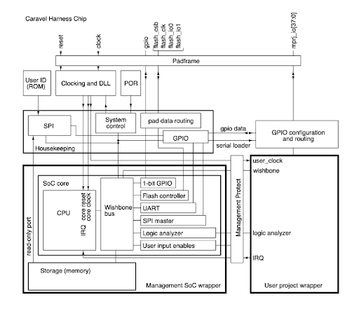
Caravel
Caravel is a template SoC (System-on-Chip) for Efabless Open MPW (Multi Project Wafer) and chipIgnite shuttles based on the OpenPDK Sky130 node and GF180MCU node.
Features of Caravel
Caravel consists of the harness frame and two main areas, which are wrappers for drop-in modules, namely, the management area and the user project area. Users place their designs in the user project area and use the management area and the padframe to receive and send signals.
- Harness frame: Contains the clocking module, DLL, user ID, housekeeping SPI, POR, and GPIO control.
- Management area: Implemented as a RISC-V-based SoC. It has peripherals such as UART, timers, and GPIO. It runs firmware which can be used to configure I/O pads and can be used to control the user project area signals and power supply.
- User project area: It has a limited silicon area of 2.92mm x 3.52mm, 38 I/O pads, 4 power domains, logic analyser probes to observe signals, and a wishbone to communicate with the management area.
You can refer to the caravel documentation for more information.
Integrating the custom RTL design with the Caravel Template
RTL Code Integration
- Clone the Caravel template from GitHub, obtaining user_project_wrapper and user_proj_example.
- User-defined modules are instantiated in user_project_wrapper to manage port interactions.
- Set up essential variables and integrate the user module’s RTL files into user_proj_example.v
- You need to modify the configs file in OpenLane based on your custom design specifications.
- Run the OpenLane flow to harden the macro.
Refer to this for a more detailed explanation
Here is a cool video by Samsung explaining how an IC fab works
Verification of the Design (testbench, Cocotb)
There are two ways we can verify the design.
- The first method involves writing a Verilog-based testbench and simulating the complete design. This process aims to validate functional verification by analyzing the produced waveforms.
- The second method utilises the Python-based testbench cocotb (coroutine-based co-simulation testbench) to verify the functional correctness of the design. It supports VHDL and SystemVerilog RTL and is known for its simplicity and versatility in the testbench environment.
Running MPW Precheck Locally
Efabless shuttle has various requirements to be met for the submission and ensure that the design meets the specified criteria and standards before being included in a multi-project wafer run. This precheck process helps identify and rectify any issues or discrepancies in the design, ensuring that it aligns with the requirements of the fabrication process.
How to submit to Efabless?
- Firstly, we need to ensure that all our codes are made public on GitHub.
- We need to login into the efabless website, select the shuttle, and then click on the “Start Project” button.
- Fill in the necessary details and an empty efabless repository will be created automatically.
We need to push our files to this repository and it can only be done through SSH linked to our profile. We can make use of git LFS (large file storage) to store the larger files that get generated during OpenLane flow.
- Create an SSH key and add it to your profile on the efabless website.
- Copy the SSH link of the empty efabless repository and add it as the remote in your local git repository.
- SSH git-lfs to track all the large files that we want to push.
- Use the added remote to push the files to the efabless repository.
Congratulations! You have successfully submitted to the efabless.
Our Submission
Great job if you’ve made it to the end of this blog! The IRIS Labs Hardware team made a submission to the previous Efabless MPW shuttle. Here’s the link to our submission under GFMPW-1 Shuttle.
IRIS Labs Lead 2023-24